Expedition PCB introduction
This lab is designed to teach you the basic workflow for creating a simple printed circuit board using the Mentor Graphics Expedition PCB tools. You will be looking at editor environments and fundamental library concepts. You will learn how to create padstacks and cells. You will eventually assemble databases for creating parts.
Schedule
Lab 1 (4 hours)
- Introduction to Expedition PCB
- LIBRARY & DATA OVERVIEW (15 min)
- CREATING PADSTACKS : exercise (45 min)
- CREATING CELLS : exercise (45 min)
- CREATING SYMBOLS : exercise (15 min)
- CREATING PARTS : exercise (30 min)
- CREATING A CUSTOM LAYOUT TEMPLATE : exercise (15 min)
Introduction to Expedition PCB
Open the dashboard application /prog/mentor/ee2007.7/2007.7EE/SDD_HOME/common/linux/bin/dash & . The left panel (Shortcuts) is for placing shortcuts to applications. Drag the ExpeditionPCB, ePlanner, DxDesigner, and Library Manager icons to the Shortcuts area from the Toolboxes directories. Expedition PCB is the High-Speed (HS) layout tool. ePlanner is the tool for setting up the HS constraints. DxDesigner is the schematic capture tool, while the Library Manager allows you to create pad stacks, cells, symbols, and parts. Your projects will listed as they are created.
PART 1 PADSTACK DEFINITION
- Open the “Library Manager” and create a new library for example under directory $HOME/kurs/lab1. What you do is to create a new directory $HOME/kurs/lab1/ and the library manager will create a number of files and directories in there.
- Click on the “Setup” menu and select “Partition Editor”, or use the buttons under the menus. See that there are initially only 25 symbols declared and no cells, no PDBs and no IBIS models. Click on “cancel”.
- You can always chose between menus and buttons.
- Under “Setup” select “Setup Parameters”. See that under “General” nothing is declared, but under “Via Definitions” there is only one standard padstack declared called “L: 026VIA”. Select “close”.
- Select the button “Library Services”. Select “Padstacks” menu and select with the browser for the “input from” to “/heim/kjetil/mgc/phys321.lmc”. Click on “open”.
- Select from “Padstacks in import partition” the “IPC, SOIC” and "Pad Round 64, Hole Rnd 41" padstacks. Be sure you select mode = “copy”. Press the “right arrow” and then “apply”. See that in the left table, the imported padstacks (for example the “IPC, SOIC”) will have a blue color. Select “close”.
- Select in the "Library Navigator Tree" the “Padstacks" item (folder). You should now have two padstack declarations under item "All". Examine the properties of both padstack declarations by double clicking on one of them.
- Examine the menus “Pads” and “Holes” from the “Padstack Editor”. Click in the menus once on the declared names listed and examine their declarations.
Exercise
Create a padstack definition for the through hole via with min. 250 μm and pad min. 450 μm (Hint: define first the “hole” and then the “pads” you need. Finally create the “padstack” with the newly declared “hole” and “pads” definitions.)
Summary
You now have learned how to create your own library; copy padstack definitions from other libraries and create your own padstacks with help of documents you get from the PCB manufacturer.
PART 2 CREATING NEW CELLS
You should have the “lab1” Library open in the Library Manager.
- Right-click on the "Cells" folder in the Library Navigator Tree.
- Create a new “Partition” called “amplifiers”.
- Right-click on the "amplifiers" section and select "New Cell".
- Enter the Cell name "8SO".
- Specify a Total number of pins of 8. Specify a Layers while editing cell of 4. Choose the IC – SOIC Package group.
- Click the "Cell Properties" button. Enter a description of SOIC 8. Set the Units to mm. Specify a Height of 1.75.
- On the Package Cell Properties dialogue, <click> the Close button.
- On the Create Package Cell dialogue, <click> the Next button and the Cell Editor tool should open.
- On the Place Pins dialogue, click the Pin # column until the pins are sorted from 1 to 8.
- Select the Padstack Name field for pin 1. Press and hold the <Shift> key then select the Padstack Name field for pin 8.
- Continuing to hold the Shift key, click the down arrow in the Padstack Name field for pin 8, and choose the SOIC padstack from the pulldown list. It should now be assigned to all of the pins.
- Click the Pattern Place tab.
- Set the Pattern type to SOIC and enter the following values into the pattern form:
- Body length = 5
- Body width = 3
- Pin to pin spacing = 1.27
- Row to row spacing = 5.2
- Make sure the Include Assembly outline and Include Silkscreen outline option are checked.
- With the pins still selected, <click> the Place button.
- Click the Close button on the Place Pins dialogue.
- Examine the graphics. Select File>Save from the menus and then select File>Exit Graphics from the menus.
- Click the S80 symbol to examine the Preview of the new cell.
- Click the New Cell button.
- Enter the Cell name 8DIP.
- Set the Total number of pins to 8. Set the Layers while editing cell to 4. Choose the IC - DIP Package group.
- Click the Cell Properties button. Enter a description of DIP 8. Verify that the Units is set to th.(=mil) Specify a Height of 100. Click the Close button.
- On the Create Package Cell dialog, click the Next button.
- Move the Place Pins dialog out of the way.
- In the graphics environment, select Setup > Editor Control from the menus.
- Select the Grids tab. Specify a Route grid of 25 and a Drawing grid of 25.
- On the Place Pins dialogue, select the Padstack Name field for pin 1. Press and hold the <Shift> key then select the Padstack Name field for pin 8.
- Continuing to hold the <Shift> key, <click> the down arrow in the Padstack Name field for pin 8 and choose the through via Pad Round 65, Hole Rond 41 (the one from previous exercise) from the pulldown list. It should then be assigned to all of the pins.
- Click the Parameter Place tab and enter the following values:
- Columns: 4 Spacing: 100
- Rows: 2 Spacing: 300
- Pin Sequence = first option.
- Click the Place button.
- Position the cursor over the drawing area. The pins are attached to the cursor for placement. Click directly on the “origin” marker to place them down.
- Select View>Fit All from the menus.
- Select Edit>Place>Assembly Outline from the menus. Using the Rectangle draw tool, draw a rectangle inside of all the pins. Draw any other assembly graphics you desire by selecting another draw tool.
- Select Edit>Place>Silkscreen Outline from the menus. Draw a rectangle outside of all the pins. Draw any other silkscreen graphics you desire.
- Select Edit>Place>Placement Outline. Draw a rectangle a little larger than the silkscreen outline.
- Move Reference Designator and Part Number text as desired by first selecting the text, positioning the mouse cursor over the text border until a “move” cursor appears, then click-drag the text.
- Select Edit>Place>Silkscreen Ref Des from the menus and place the text outside of the silkscreen outline.
- Select File>Save from the menus.
- Select File>Exit Graphics from the menus.
- Select each cell in the list to see a Preview of it.
PART 3 CREATING SYMBOLS
You should have the “lab1” Central Library open in the Library Manager.
- Right-click on the "Symbols" folder in the Library Navigator Tree.
- Create a new “Partition” called “amplifiers”.
- Right-click on the "amplifiers" folder under the "Symbols" folder in the Library Navigator Tree.
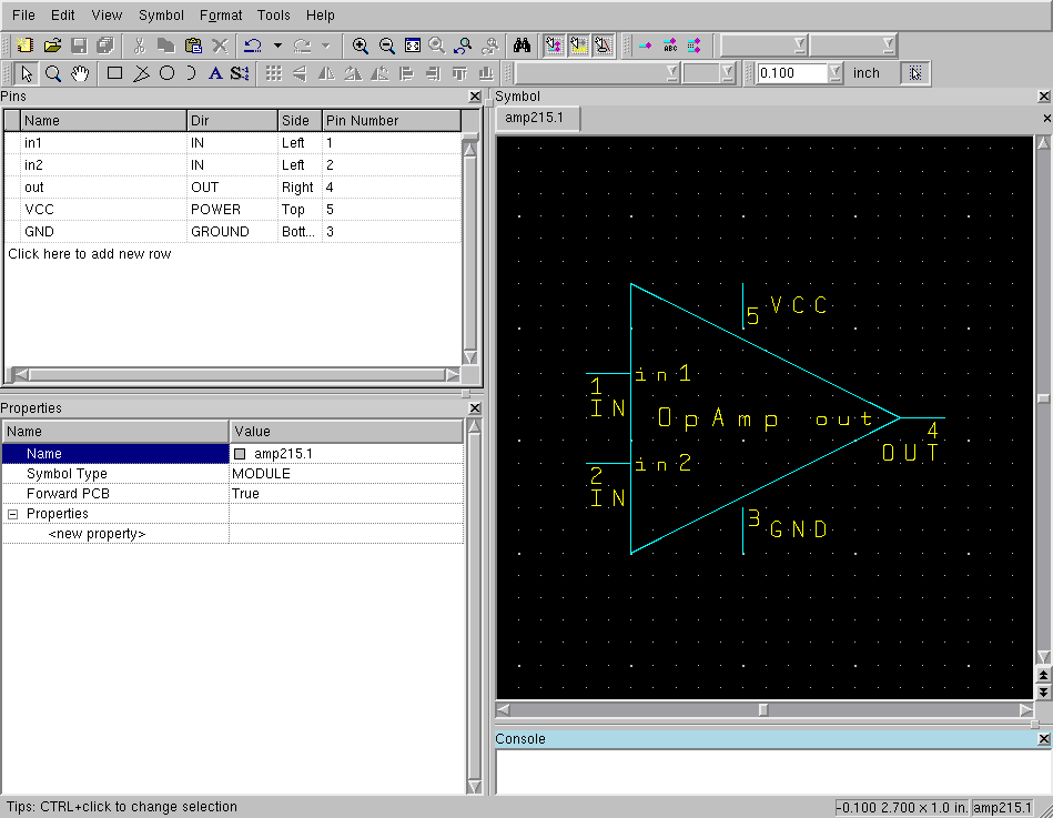
- Create a new “Symbol” called “amp215”. (A graphical editor should pop-up.)
- Examine the window and create the opamp as pictured below: (don’t forget to give the pins properties e.g. “input” property or “output” property.)
- Save your work and exit the “Symbol Editor”. During “saving”, the design is checked against DRC rules.

PART 4 CREATING PARTS
You should have the “lab1” Central Library open in the Library Manager.
- Right-click on the "Parts" folder in the Library Navigator Tree.
- Create a new “Partition” called “amplifiers”.
- Right-click on the "amplifiers" folder under the "Parts" folder in the Library Navigator Tree.
- Create a new “Part” called “amp01”. (The Part Editor dialogue should pop-up.)
- Change the Number to "Opamp1". Change the Label to "amp01A".
- At the lower-left corner of the PartsDB Editor dialog, verify that the Component property value for Type is IC.
- Enter the Description of IC, "A single amplifier packaged".
- Specify a Reference des prefix of "U".
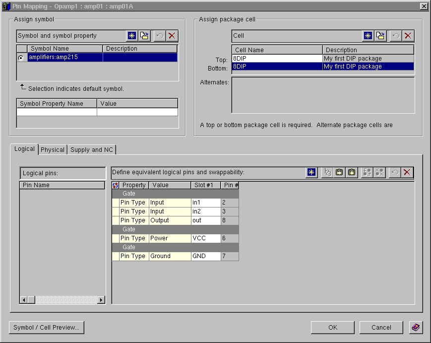
- On the Part Editor dialog, click the Pin Mapping button.
- In the Assign symbols section of the dialog (upper-left corner), click the Import button.
- On the Import dialog, select the symbol name amp215 from the list (select "amplifiers" from the Central Library, and then the Symbol name).
- Select Create New gate information option.
- Enter the Number of slots as 1.
- Select the Include pin properties option.
- Click the OK button. A new gate will be created in the Logical table with 4 slots.
- In the Assign package cell section of the dialog (upper-right corner), click on the Import button.
- On the Import dialog, select 8DIP from the list of cells and <click> the OK button.
- Examine the Logical table and Physical table at the bottom of the Pin Mapping dialog. The symbol imported with 1 slot defined.
- Click the Physical tab. Enter the following physical pin outs:
- In1 2
- In2 3
- VCC 6
- GND 7
- Out 8
- Click the Supply and NC tab.
- Enter a Pin # of 1,4,5 for NC.
- Click the OK button on the Pin Mapping dialog to save your work.
- Select File>Save from the menus.
- Exit the Part Editor.

PART 5 CREATING A LAYOUT TEMPLATE
You should have the “lab1” Central Library open in the Library Manager.
- Click button “layout templates”.
- Click once on the “4 layer Template” and press the “copy template” button above.
- Click once on the copied template and give it the name “lab1 template”.
- Click once on the “edit template” button. A default template is opened in “Expedition PCB”.
- Click on the menu “Setup>Setup Parameters”.
- In the “General” tap set the “number of physical layers” to 6. “Display units” should be set to “microns” and “meters/s”. Click on “Apply”.
- In the “Layer Stackup” tab change for all dielectric layers thickness the value to “500 um”. Make sure you select the option “keep layer stackup in sync with layer def. In Planes tab.”
- Select “OK”.
- “Save” the template and “exit”.
