Layout XL and IHP SG13S: Difference between revisions
No edit summary |
No edit summary |
||
| Line 45: | Line 45: | ||
== DRD == | == DRD == | ||
[[File:DRDbuttons.png|50px]] | [[File:DRDbuttons.png|50px]] | ||
DRD stands for Dynamic Design Rule Checking and are helpful while laying out your design. DRD Enforce On prevents you from doing anything that breaks the rules, and DRD Notify tells you if what you are doing is illegal. Image below shows example of DRD Notify. | DRD stands for Dynamic Design Rule Checking and are helpful while laying out your design. DRD Enforce On prevents you from doing anything that breaks the rules, and DRD Notify tells you if what you are doing is illegal. Image below shows example of DRD Notify. | ||
[[File:DRD.png|200px]] | [[File:DRD.png|200px]] | ||
== Drawing == | |||
To draw rectangles (e.g. NWell) choose the wanted layer on the left side then press R. To create a connection between to nodes you can either create a wire (Ctrl+W) or a path (P). A wire automatically helps with choosing layer, and may also be used to create vias to another layer by left-clicking. | |||
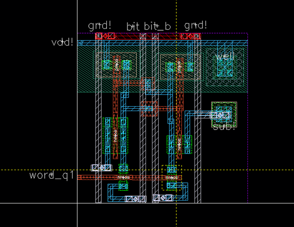
A complete layout could look something like this: | |||
[[File:sram.png|600px]] | |||
= DRC = | |||
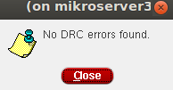
Run DRC by pressing Assura -> Run DRC. Make sure technology is SG13_dev and the Rule Set is default. Read about the different switches in the user guide (e.g. antenna-rules etc). If everything is ok this message should appear: | |||
[[File:drcok.png|200px]] | |||
The DRC should also be run for Rule Set: Fill and Density. | |||
= LVS = | |||
Run LVS by pressing Assura -> Run LVS. | |||
Revision as of 11:05, 12 April 2016
Before starting layout
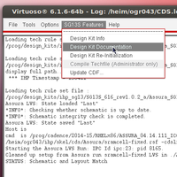
Read the Design Kit User Guide. Especially the part of connecting the substrate (chapter 8.2) and layout (chapter 9). Also make sure you understand the Layout Rules document.
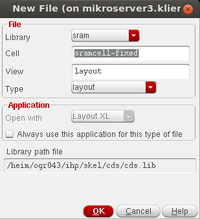
If your laying out just one cell (in our case a SRAM-cell) make sure it contains defined values and not just pPar("")-values. This makes it easier to produce the right transistor-sizes etc. If you do not want to change your schematic, make a copy to another cell (e.g. from "sram" to "sram-fixed").
Layout XL
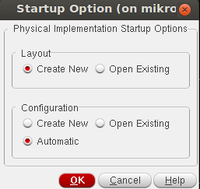
From the schematic click Launch -> Layout XL to open the layout environment.
Layout XL opens with a new black empty canvas. The schematic window also opens. This is very useful as when we add our devices in the layout we can see which device they represent in the schematic as they get highlighted.
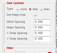
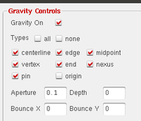
Before anything you must define some options to avoid a lot of DRC-errors down the line. In the Layout Rules-document we read what our drawing-grid restrictions are (bottom of page 10). In Layout XL press E to open the Display Options-window. Remember that all size-values are in micrometers. Set the X and Y Snap Spacing to reflect the grid rules. Now press Shift-E to open the Layout Editor Options. Set gravity on(you can turn this off later with the g-key if you dont like it), and aperture around 0.1. This defines the the distance before snapping to another object etc.
Generate from source
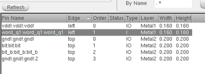
IHP has already defined transistors, pins, etc. for different sized, so it is not needed to draw these from scratch. You should, however, dissect them to understand how they work. To place all the devices from the schematic press Connectivity -> Generate -> All From Source. In this window we define which of our devices we want to place, the I/O pins, PR boundary (the area which our cell must be within) and floorplan settings (if needed). For our cell we need to change the IO-pins. We want the gnd and bit-lines to be vertical, and vdd and word-lines to be horizontal. This means that they will intersect each other and must be in different layers. We also want two gnd-pins which also can be defined here. Remember to uncheck Create under the sub!-pin since this is not needed.
Change the Label options to a smaller font size (about 0.1 is ok). Click OK to see the results.
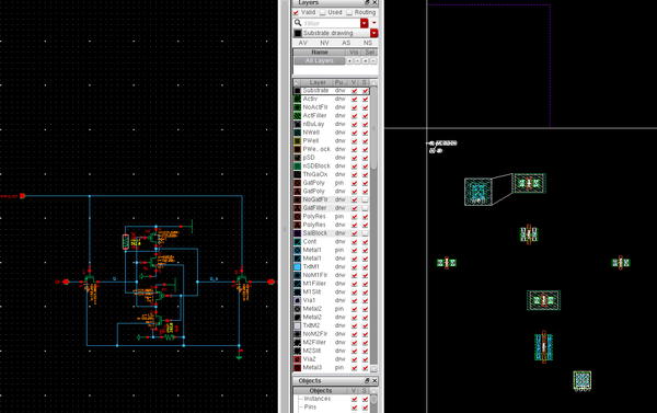
The purple box is the PR boundary in which are layout must be contained. Notice how the ntap1 is highlighted in the schematic when clicked in the layout window.
Pin Placement
Press Place -> Pin Placement. This opens a windows that lets us define the position of our pins. This is very helpful to line up our design. Remember that the positions may be tweaked later.
Placing devices
If you are extremely lazy you can autoplace the components with Place -> Custom Digital -> Placer. This, however, will probably not give you the desired result. To help you place the the devices correctly it is helpful to see which devices that connect to each other and how. This is accomplished with Connectivity -> Nets -> Show/Hide All Incomplete Nets. This will give you a all the nets that are uncompleted and can be very daunting. However, you can use Ctrl++ (that is Ctrl and +-key ) to turn on or off the nets for the selected device.
F4 switches between Full and Partial Select. Partial Select means that we are able to select individual pieces of a device, e.g. if we want to stretch a part.
DRD
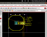
DRD stands for Dynamic Design Rule Checking and are helpful while laying out your design. DRD Enforce On prevents you from doing anything that breaks the rules, and DRD Notify tells you if what you are doing is illegal. Image below shows example of DRD Notify.
Drawing
To draw rectangles (e.g. NWell) choose the wanted layer on the left side then press R. To create a connection between to nodes you can either create a wire (Ctrl+W) or a path (P). A wire automatically helps with choosing layer, and may also be used to create vias to another layer by left-clicking.
A complete layout could look something like this:
DRC
Run DRC by pressing Assura -> Run DRC. Make sure technology is SG13_dev and the Rule Set is default. Read about the different switches in the user guide (e.g. antenna-rules etc). If everything is ok this message should appear:
The DRC should also be run for Rule Set: Fill and Density.
LVS
Run LVS by pressing Assura -> Run LVS.
