SmartFusion2- AMBA APB, Custom Peripheral: Difference between revisions
No edit summary |
No edit summary |
||
| (One intermediate revision by the same user not shown) | |||
| Line 192: | Line 192: | ||
Go to ''Project'', ''Project Settings'', ''Device I/O Settings'' and set ''Default I/O Technology'' to ''LVCMOS 3.3V''. | Go to ''Project'', ''Project Settings'', ''Device I/O Settings'' and set ''Default I/O Technology'' to ''LVCMOS 3.3V''. | ||
Import the Physical Design Constraint file supplied below. Name it Fabric_top. | Import the Physical Design Constraint file supplied below. Name it Fabric_top.pdc. | ||
# Microsemi I/O Physical Design Constraints file | # Microsemi I/O Physical Design Constraints file | ||
| Line 762: | Line 762: | ||
reset_n : in std_logic; -- asynch reset, negative polarity | reset_n : in std_logic; -- asynch reset, negative polarity | ||
global_reset : in std_logic; -- global reset, positive polarity | global_reset : in std_logic; -- global reset, positive polarity | ||
rcu_reset : in std_logic; -- reset for RCU Xilinx fw, positive polarity | rcu_reset : in std_logic; -- reset for RCU Xilinx fw, positive polarity | ||
Latest revision as of 12:50, 22 October 2013
Intro
This tutorial explains how to implement and test a custom AMBA APB (Advanced Peripheral Bus) module. The tutorial will create a SmartFusion2 MSS (Microcontroller Subsystem) with APB bus interface. The custom module will be connected to the APB bus to map from APB bus to a DCS bus. Connected to the DCS part there will be a test module, which you can write and read from. The MSS will also have a GPIO module connected to a LED and serial UART peripheral.
Before you start
Make sure you have installed Libero and have a valid license, as described in SmartFusion2. This tutorial assumes Libero v11.1 is used and that you are using the SmartFusion2 starter kit from Microsemi.
Create new project
Start Libero SoC v11.1. Press Project and New Project. Name your project APB_custom_peripheral. Use system tools SmartFusion2 Microcontroller Subsystem (MSS). 
Modify MSS
Double click on the MSS component to modify it. A new window will open. Enable/Disable peripherals until your MSS looks like the image below.
Tip: click View > Maximize Work Area or CTRL+W to expand the working area while enabling and disabling the MSS peripherals.

Click on the configuration button for the enabled peripherals, and configure them like the following images
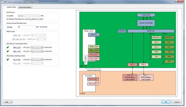
MSS CCC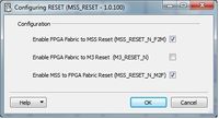
Reset Controller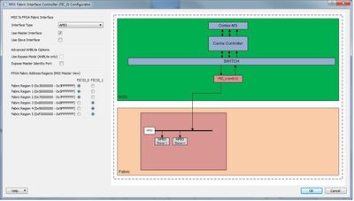
FIC 0
MMUART 0
Your MSS should now look like this: 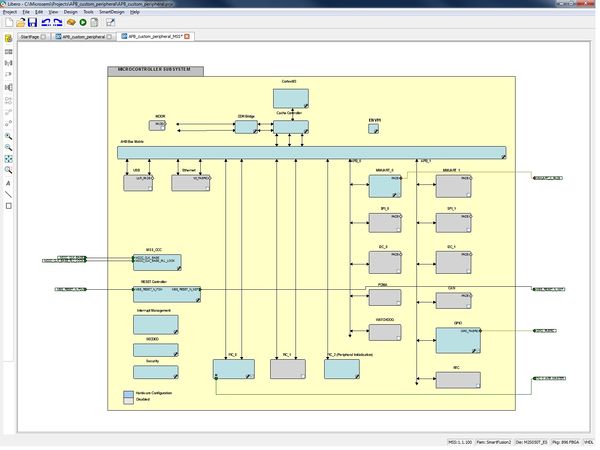
SmartDesign
Close the MSS configuration window. On the SmartDesign canvas, right click on the MSS component and Update instance(s) with Latest Component.
From Catalog add the following components:
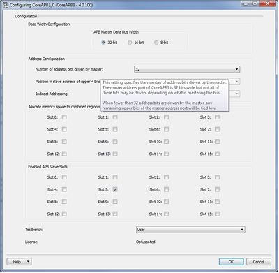
CoreAPB3 from Bus Interfaces,
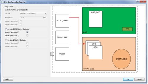
Chip Oscillators and Clock Conditioning Circuitry from Clock & Management
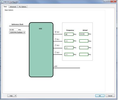
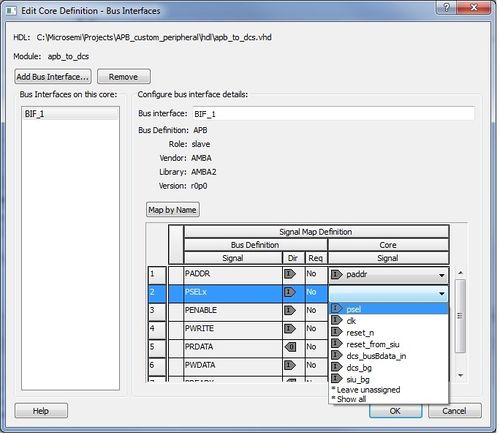
Now import all the vhdl files which are included at the bottom of the page. Save the files with the names specified in the text. The files can be included by clicking File, Import, HDL Source Files. These files can now be found under hdl in the Files tab and in Design Hierarchy. In Design Hierarchy right click on DCS_test, choose Create Core from HDL. Answer No to question about adding bus interfaces to core. Right click on apb_to_dcs and choose Create Core from HDL. Choose Yes on question about adding bus interfaces to core. Choose Add/Edit bus interfaces.... In next window, click Add Bus Interface..., choose APB, AMBA, AMBA2, slave. Connect PSELx to psel.
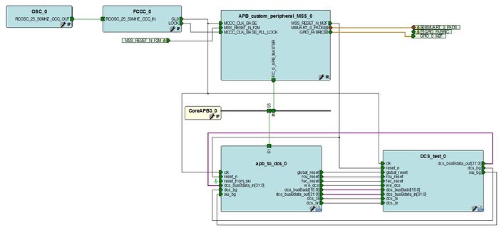
Add the modules you made to the SmartDesign. In design canvas, right click and choose Auto Connect followed by Auto Arrange Instances. Right click on MSS_RESET_N_F2M and GPIO_FABRIC and select Promote to Top Level. Right click on reset_from_siu and choose Tie Low. Connect the unconnected wires. The result should look something like the image below
Generate component by clicking SmartDesign and Generate Component.
Pre-synthesized Simulation
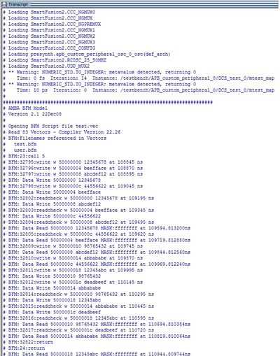
To simulate the functionality of the abp_to_dcs module, normal APB bus functionality from the MSS should be used. To do this you can add a .bfm file (Bus Functional Model). Copy the following to the User.bfm in your project, located under Files and simulation.
#===========================================================
# Enter your BFM commands in this file.
#
# Syntax:
# -------
#
# memmap    resource_name base_address;
#
# write     width resource_name byte_offset data;
# read      width resource_name byte_offset;
# readcheck width resource_name byte_offset data;
#
#===========================================================

#include "subsystem.bfm"

procedure user_main;

# perform subsystem initialization routine
#  call subsystem_init;

# add your BFM commands below:

memmap apb_to_dcs_0 0x50000000;


write w apb_to_dcs_0 0x0 0x12345678;
write w apb_to_dcs_0 0x4 0xBEEFFACE;
write w apb_to_dcs_0 0x8 0xABCDEF12;
write w apb_to_dcs_0 0xC 0x44556622;


readcheck w apb_to_dcs_0 0x0 0x12345678;
readcheck w apb_to_dcs_0 0x4 0xBEEFFACE;
readcheck w apb_to_dcs_0 0x8 0xABCDEF12;
readcheck w apb_to_dcs_0 0xC 0x44556622;


write w apb_to_dcs_0 0x10 0x98765432;
write w apb_to_dcs_0 0x14 0xABBABABE;
write w apb_to_dcs_0 0x18 0x12345ABC;
write w apb_to_dcs_0 0x1C 0xDEADBEEF;

readcheck w apb_to_dcs_0 0x10 0x98765432;
readcheck w apb_to_dcs_0 0x14 0xABBABABE;
readcheck w apb_to_dcs_0 0x18 0x12345ABC;
readcheck w apb_to_dcs_0 0x1C 0xDEADBEEF;


return
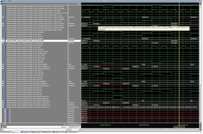
Next, go to Project and then Project Settings. Choose DO File under Simulation Options. You can use the run.do file supplied below. If you want to use automatic .do file and add signals yourself you can use standard settings, but be sure to change simulation time to 150 us. The system has got some initialization time, which takes around 120 us with this setup, before the bus signals start to change.
quietly set ACTELLIBNAME SmartFusion2
quietly set PROJECT_DIR "C:/Microsemi/Projects/APB_custom_peripheral"
source "${PROJECT_DIR}/simulation/CompileDssBfm.tcl";source "${PROJECT_DIR}/simulation/bfmtovec_compile.tcl";

if {[file exists presynth/_info]} {
   echo "INFO: Simulation library presynth already exists"
} else {
   vlib presynth
}
vmap presynth presynth
vmap SmartFusion2 "C:/Microsemi/Libero_v11.1/Designer/lib/modelsim/precompiled/vhdl/SmartFusion2"
if {[file exists COREAPB3_LIB/_info]} {
   echo "INFO: Simulation library COREAPB3_LIB already exists"
} else {
   vlib COREAPB3_LIB
}
vmap COREAPB3_LIB "COREAPB3_LIB"

vcom -93 -explicit  -work presynth "${PROJECT_DIR}/component/work/APB_custom_peripheral_MSS/APB_custom_peripheral_MSS.vhd"
vcom -93 -explicit  -work presynth "${PROJECT_DIR}/hdl/dcs_interface_pkg.vhd"
vcom -93 -explicit  -work presynth "${PROJECT_DIR}/hdl/apb_to_dcs.vhd"
vcom -93 -explicit  -work presynth "${PROJECT_DIR}/hdl/mtest.vhd"
vcom -93 -explicit  -work presynth "${PROJECT_DIR}/hdl/DCS_test.vhd"
vcom -93 -explicit  -work presynth "${PROJECT_DIR}/component/work/APB_custom_peripheral/FCCC_0/APB_custom_peripheral_FCCC_0_FCCC.vhd"
vcom -93 -explicit  -work presynth "${PROJECT_DIR}/component/work/APB_custom_peripheral/OSC_0/APB_custom_peripheral_OSC_0_OSC.vhd"
vcom -93 -explicit  -work COREAPB3_LIB "${PROJECT_DIR}/component/Actel/DirectCore/CoreAPB3/4.0.100/rtl/vhdl/core_obfuscated/coreapb3_muxptob3.vhd"
vcom -93 -explicit  -work COREAPB3_LIB "${PROJECT_DIR}/component/Actel/DirectCore/CoreAPB3/4.0.100/rtl/vhdl/core_obfuscated/coreapb3_iaddr_reg.vhd"
vcom -93 -explicit  -work COREAPB3_LIB "${PROJECT_DIR}/component/Actel/DirectCore/CoreAPB3/4.0.100/rtl/vhdl/core_obfuscated/coreapb3.vhd"
vcom -93 -explicit  -work COREAPB3_LIB "${PROJECT_DIR}/component/Actel/DirectCore/CoreAPB3/4.0.100/rtl/vhdl/core_obfuscated/components.vhd"
vcom -93 -explicit  -work presynth "${PROJECT_DIR}/component/work/APB_custom_peripheral/APB_custom_peripheral.vhd"
vcom -93 -explicit  -work presynth "${PROJECT_DIR}/component/work/APB_custom_peripheral/testbench.vhd"

vsim -L SmartFusion2 -L presynth -L COREAPB3_LIB  -t 1fs presynth.testbench

add wave  \
sim:/testbench/APB_custom_peripheral_0/APB_custom_peripheral_MSS_0/FIC_0_APB_M_PREADY \
sim:/testbench/APB_custom_peripheral_0/APB_custom_peripheral_MSS_0/FIC_0_APB_M_PSLVERR \
sim:/testbench/APB_custom_peripheral_0/APB_custom_peripheral_MSS_0/MCCC_CLK_BASE \
sim:/testbench/APB_custom_peripheral_0/APB_custom_peripheral_MSS_0/MCCC_CLK_BASE_PLL_LOCK \
sim:/testbench/APB_custom_peripheral_0/APB_custom_peripheral_MSS_0/MSS_RESET_N_F2M \
sim:/testbench/APB_custom_peripheral_0/APB_custom_peripheral_MSS_0/FIC_0_APB_M_PADDR \
sim:/testbench/APB_custom_peripheral_0/APB_custom_peripheral_MSS_0/FIC_0_APB_M_PENABLE \
sim:/testbench/APB_custom_peripheral_0/APB_custom_peripheral_MSS_0/FIC_0_APB_M_PSEL \
sim:/testbench/APB_custom_peripheral_0/APB_custom_peripheral_MSS_0/FIC_0_APB_M_PWDATA \
sim:/testbench/APB_custom_peripheral_0/APB_custom_peripheral_MSS_0/FIC_0_APB_M_PRDATA \
sim:/testbench/APB_custom_peripheral_0/APB_custom_peripheral_MSS_0/FIC_0_APB_M_PWRITE \
sim:/testbench/APB_custom_peripheral_0/APB_custom_peripheral_MSS_0/MSS_RESET_N_M2F
add wave  \
sim:/testbench/APB_custom_peripheral_0/apb_to_dcs_0/penable \
sim:/testbench/APB_custom_peripheral_0/apb_to_dcs_0/psel \
sim:/testbench/APB_custom_peripheral_0/apb_to_dcs_0/pwrite \
sim:/testbench/APB_custom_peripheral_0/apb_to_dcs_0/paddr \
sim:/testbench/APB_custom_peripheral_0/apb_to_dcs_0/pwdata \
sim:/testbench/APB_custom_peripheral_0/apb_to_dcs_0/prdata \
sim:/testbench/APB_custom_peripheral_0/apb_to_dcs_0/pslverr \
sim:/testbench/APB_custom_peripheral_0/apb_to_dcs_0/clk \
sim:/testbench/APB_custom_peripheral_0/apb_to_dcs_0/reset_n \
sim:/testbench/APB_custom_peripheral_0/apb_to_dcs_0/reset_from_siu \
sim:/testbench/APB_custom_peripheral_0/apb_to_dcs_0/global_reset \
sim:/testbench/APB_custom_peripheral_0/apb_to_dcs_0/rcu_reset \
sim:/testbench/APB_custom_peripheral_0/apb_to_dcs_0/fec_reset \
sim:/testbench/APB_custom_peripheral_0/apb_to_dcs_0/we_dcs \
sim:/testbench/APB_custom_peripheral_0/apb_to_dcs_0/pready \
sim:/testbench/APB_custom_peripheral_0/apb_to_dcs_0/dcs_busBadd \
sim:/testbench/APB_custom_peripheral_0/apb_to_dcs_0/dcs_busBdata_in \
sim:/testbench/APB_custom_peripheral_0/apb_to_dcs_0/dcs_busBdata_out \
sim:/testbench/APB_custom_peripheral_0/apb_to_dcs_0/dcs_bi \
sim:/testbench/APB_custom_peripheral_0/apb_to_dcs_0/dcs_bg \
sim:/testbench/APB_custom_peripheral_0/apb_to_dcs_0/dcs_br \
sim:/testbench/APB_custom_peripheral_0/apb_to_dcs_0/siu_bg
add wave  \
sim:/testbench/APB_custom_peripheral_0/DCS_test_0/we_dcs \
sim:/testbench/APB_custom_peripheral_0/DCS_test_0/dcs_busBadd \
sim:/testbench/APB_custom_peripheral_0/DCS_test_0/dcs_busBdata_in \
sim:/testbench/APB_custom_peripheral_0/DCS_test_0/dcs_busBdata_out \
sim:/testbench/APB_custom_peripheral_0/DCS_test_0/dcs_bi \
sim:/testbench/APB_custom_peripheral_0/DCS_test_0/dcs_bg \
sim:/testbench/APB_custom_peripheral_0/DCS_test_0/dcs_br \
sim:/testbench/APB_custom_peripheral_0/DCS_test_0/siu_bg \
sim:/testbench/APB_custom_peripheral_0/DCS_test_0/mtest_map/wr_en \
sim:/testbench/APB_custom_peripheral_0/DCS_test_0/mtest_map/rd_en \
sim:/testbench/APB_custom_peripheral_0/DCS_test_0/mtest_map/address \
sim:/testbench/APB_custom_peripheral_0/DCS_test_0/mtest_map/data_in \
sim:/testbench/APB_custom_peripheral_0/DCS_test_0/mtest_map/data_out \
sim:/testbench/APB_custom_peripheral_0/DCS_test_0/mtest_map/myram
run 150 us
Double click on Simulate in Design Flow under Verify Pre-Synthesized Design which will start ModelSim.
Constraints, Synthesize and Place&Route
Go to Project, Project Settings, Device I/O Settings and set Default I/O Technology to LVCMOS 3.3V.
Import the Physical Design Constraint file supplied below. Name it Fabric_top.pdc.
# Microsemi I/O Physical Design Constraints file
# Auto Generated User I/O Constraints file

# Version: v11.1 11.1.0.14
# Family: SmartFusion2 , Die: M2S050T_ES , Package: 896 FBGA
# Date generated: Fri Sep 20 10:03:27 2013


#
# User Locked I/O Bank Settings
#
set_iobank Bank0 -vcci 1.80 -fixed yes
set_iobank Bank1 -vcci 3.30 -fixed yes
set_iobank Bank2 -vcci 3.30 -fixed yes
set_iobank Bank3 -vcci 3.30 -fixed yes
set_iobank Bank4 -vcci 3.30 -fixed yes
set_iobank Bank8 -vcci 3.30 -fixed yes

#
# Unlocked I/O Bank Settings
# The I/O Bank Settings can be locked by directly editing this file
# or by making changes in the I/O Attribute Editor
#


#
# User Locked I/O settings
#
set_io MMUART_0_RXD -pinname L23 -fixed yes
set_io MMUART_0_TXD -pinname H27 -fixed yes


set_io MSS_RESET_N_F2M  \
    -pinname F30        \
    -fixed yes          \
    -RES_PULL Up        \
    -DIRECTION INPUT


set_io GPIO_0_M2F            \
    -pinname G30       \
    -fixed yes         \
    -DIRECTION OUTPUT
The file is imported by clicking File, Import, I/O Constraints (PDC) Files. Once this is included, scroll in Design Flow to Place and Route and right click. Select Configure Options and uncheck Timing Driven.
Now you can click on the "Play" button, Generate Programming Data. This process will take some time. If all succeeds, you should be able to program your FPGA. Program it by connecting power and FlashPro Programmer and click on Run Programming Action.
Create Test Software
To write test application software, scroll to the bottom of the Design Flow and click Write Application Code. This will open SoftConsole from Microsemi. You can replace the main.c with the following:
#include "unistd.h"
#include <stdio.h>
#include "drivers/mss_uart/mss_uart.h"
#include "drivers/mss_gpio/mss_gpio.h"


//Initialize registers to read/write
#define APB_TO_DCS_0                    0x50000000U
#define MEM1 		(*(volatile int32_t *) 0x50000000)
#define MEM2 		(*(volatile int32_t *) 0x50000004)
#define MEM3 		(*(volatile int32_t *) 0x50000008)
#define MEM4 		(*(volatile int32_t *) 0x5000000C)
#define MEM5 		(*(volatile int32_t *) 0x50000010)
#define MEM6 		(*(volatile int32_t *) 0x50000014)
#define MEM7 		(*(volatile int32_t *) 0x50000018)
#define MEM8 		(*(volatile int32_t *) 0x5000001C)

//Define a constant delay value
#define DELAY_LOAD_VALUE	0x00080000     			//about half a second


int main()
{
/*
* Initialize MSS GPIOs.
*/
MSS_GPIO_init();

/*
 * Configure MSS GPIO pin
 */
MSS_GPIO_config( MSS_GPIO_0 , MSS_GPIO_OUTPUT_MODE );

/*
 * Set initial state of GPIO pin
 */
MSS_GPIO_set_output(MSS_GPIO_0,0);


//Using UART 0
mss_uart_instance_t * const gp_my_uart = &g_mss_uart0;

/*
 * Using one delay to write and one delay to read
 */
volatile int32_t delay_count_1 = 0;
volatile int32_t delay_count_2 = 0;
delay_count_1 = DELAY_LOAD_VALUE/2;
delay_count_2 = DELAY_LOAD_VALUE;

/*
 * Variable to read value from memory to set led
 */
uint8_t led;


/*
 * Incrementing value to be written to memory
 */
int32_t i = 0;

/*
 * Variables to hold values read from memory
 */
int32_t m1,m2,m3,m4,m5,m6,m7,m8;

/*
 * data to be sent on UART, holding chopped memory data
 */
uint8_t data[4];

    /*--------------------------------------------------------------------------
     * Initialize and configure UART.
     */
    MSS_UART_init(gp_my_uart,
                  MSS_UART_57600_BAUD,
                  MSS_UART_DATA_8_BITS | MSS_UART_NO_PARITY | MSS_UART_ONE_STOP_BIT);

    MSS_UART_polled_tx_string(gp_my_uart,(const uint8_t*) "\n\r*******************Hello World*********************\n\r");

	//Always
	while( 1 )
	{
		-- delay_count_1;
		-- delay_count_2;


		/*
		 * Updating memory values
		 */
		if (delay_count_1 <= 0)
		{
			delay_count_1 = DELAY_LOAD_VALUE;
			MEM1 = i;
			MEM2 = i+1;
			MEM3 = i+2;
			MEM4 = i+3;
			MEM5 = i+4;
			MEM6 = i+5;
			MEM7 = i+6;
			MEM8 = i+7;

		}
		/*
		 * Reading memory values
		 */
		if (delay_count_2 <= 0)
		{
			delay_count_2 = DELAY_LOAD_VALUE;
			m1 = MEM1;
			if(m1 != i) {
				 MSS_UART_polled_tx_string(gp_my_uart,(const uint8_t*) "\n\r**** Data read on memory location 1 is different from expected! *****\n\r");
			}

			/*
 			 * Chopping data from memory, sending it to UART.
			 * Reading hex/binary values from console
			 */
		    data[3] = m1;
		    data[2] = m1 >>8;
		    data[1] = m1 >>16;
		    data[0] = m1 >>24;
		    MSS_UART_polled_tx(gp_my_uart, data, sizeof(data));

			m2 = MEM2;
			if(m2 != i+1) {
				 MSS_UART_polled_tx_string(gp_my_uart,(const uint8_t*) "\n\r**** Data read on memory location 2 is different from expected! *****\n\r");
			}
			m3 = MEM3;
			if(m3 != i+2) {
				 MSS_UART_polled_tx_string(gp_my_uart,(const uint8_t*) "\n\r**** Data read on memory location 3 is different from expected! *****\n\r");
			}
			m4 = MEM4;
			if(m4 != i+3) {
				 MSS_UART_polled_tx_string(gp_my_uart,(const uint8_t*) "\n\r**** Data read on memory location 4 is different from expected! *****\n\r");
			}
			m5 = MEM5;
			if(m5 != i+4) {
				 MSS_UART_polled_tx_string(gp_my_uart,(const uint8_t*) "\n\r**** Data read on memory location 5 is different from expected! *****\n\r");
			}
			m6 = MEM6;
			if(m6 != i+5) {
				 MSS_UART_polled_tx_string(gp_my_uart,(const uint8_t*) "\n\r**** Data read on memory location 6 is different from expected! *****\n\r");
			}
			m7 = MEM7;
			if(m7 != i+6) {
				 MSS_UART_polled_tx_string(gp_my_uart,(const uint8_t*) "\n\r**** Data read on memory location 7 is different from expected! *****\n\r");
			}
			m8 = MEM8;
			if(m8 != i+7) {
				 MSS_UART_polled_tx_string(gp_my_uart,(const uint8_t*) "\n\r**** Data read on memory location 8 is different from expected! *****\n\r");
			}

			/*
			 * Read last bit of current value of m1 and set GPIO (led) according to the bit value
			 * Bit should toggle for every read cycle
			 */
			led = m1 & 0x00000001;
			MSS_GPIO_set_output(MSS_GPIO_0,led);


			++i;
		}

	}
}
The application will write data to RAM and then read it. A LED is linked to the LSB of the read data, which cause the LED to blink. Data read on first memory location is written to the UART, and can be observed with a serial terminal program. Note that serial data sent on the UART is counting binary, and ASCII format is not implemented. The UART also sends out a message on the UART if the read data is different from expected.
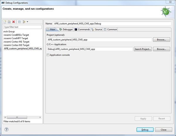
Build Debug Application by pressing Debug Configurations and then choose Microsemi Cortex M3 Target. Press Apply, build debug target and launch debug target.

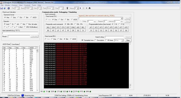
VHDL files
-------------------------------------------------------------------------------
-- Title      : APB_to_DCS
-- Project    : RCU2
-------------------------------------------------------------------------------
-- File             : apb_to_dcs.vhd
-- Last edited by   : Christian Torgersen
-- Last update      : 30.09.2013 - 09:26
-- Current Revision : 1.0
-------------------------------------------------------------------------------
-- Description      : Mapping between AMBA APB and DCS bus.
-------------------------------------------------------------------------------
-- Revision History :
-------------------------------------------------------------------------------
--
-- This file is property of and copyright by the Instrumentation and
-- Electronics Section, Dep. of Physics and Technology
-- University of Bergen, Norway
-- This file has been written by Christian Torgersen
-- Christian.torgersen@student.uib.no
--
-- Permission to use, copy, modify and distribute this firmware and its
-- documentation strictly for non-commercial purposes is hereby granted
-- without fee, provided that the above copyright notice appears in all
-- copies and that both the copyright notice and this permission notice
-- appear in the supporting documentation. The authors make no claims
-- about the suitability of this software for any purpose. It is
-- provided "as is" without express or implied warranty.
--
-------------------------------------------------------------------------------

library ieee;
use ieee.std_logic_1164.all;
use ieee.std_logic_unsigned.all;

library work;
use work.dcs_interface_pkg.all;

entity apb_to_dcs is
port(
	--APB input control signals
	penable				: in		std_logic;						-- APB enable signal. Asserted high on second pulse
	psel				: in		std_logic;						-- APB slave select from master
	pwrite				: in		std_logic;						-- APB direction setting

	--APB input and addr
	paddr				: in		std_logic_vector(31 downto 0);	-- APB address
	pwdata				: in		std_logic_vector(31 downto 0);	-- APB write data

	--APB output signals
	prdata				: out	std_logic_vector(31 downto 0);	-- APB read data
	pready				: out	std_logic;						-- APB hold signal, for read/write more than 2 cycles
	pslverr				: out	std_logic;						-- APB slave error signal

    clk                 : in    std_logic;                     -- global clock (40 MHz)
    reset_n             : in    std_logic;                     -- asynch reset, negative polarity
    reset_from_siu      : in    std_logic;                     -- asynch reset from SIU, positive polarity

	--internal resets
	global_reset        : out   std_logic;                     -- global reset, positive polarity
    rcu_reset           : out   std_logic;                     -- reset for RCU Xilinx fw,  positive polarity
    fec_reset           : out   std_logic;                     -- reset for FEC, positive polarity

	--DCS bus signals
	we_dcs              : out   std_logic;                     -- write enable to the internal modules
	dcs_busBadd         : out   std_logic_vector(15 downto 0); -- address passed through
	dcs_busBdata_in     : in    std_logic_vector(31 downto 0); -- data from internal modules to DCS
	dcs_busBdata_out    : out   std_logic_vector(31 downto 0); -- data to internal modules from DCS
	dcs_bi              : out   std_logic;                     -- interrupt in case DCS needs bus
	dcs_bg              : in    std_logic;                     -- dcs bus grant from arbiter
    dcs_br              : out   std_logic;	                   -- dcs bus request to arbiter
    siu_bg              : in    std_logic                      -- siu bus grant from arbiter
	);
end apb_to_dcs;

architecture arc of apb_to_dcs is

--signal declarations
	type   state is (s_idle, s_wait_for_grant, s_grant, s_error);
	signal current_state, next_state : state;

--	signal resetting        : std_logic; -- high when the resetting addresses are received, only used by dcs_addr
	signal timeout			:std_logic;
	signal timeout_cnt		:std_logic_vector(6 downto 0);
	signal timeout_cnt_en	:std_logic;
	signal we_dcs_i			:std_logic;

begin

--combinatorics
timeout		<= timeout_cnt(6);

we_dcs				<= we_dcs_i;
dcs_br				<= '1' when (psel = '1'and (next_state = s_wait_for_grant or next_state = s_grant)) else '0';

dcs_busBadd			<= paddr(15 downto 0);										--linking between APB and      dcs addresses
dcs_busBdata_out	<= pwdata when (pwrite='1' and dcs_bg= '1') else (others => '0');				-- APB to DCS data
prdata				<= dcs_busBdata_in when (pwrite ='0' and dcs_bg= '1') else (others => '0');		-- DCS to APB data

-- purpose: timeout counter for transaction
p_timeout_cnt: process(clk, reset_n, reset_from_siu)
begin
  if (reset_n = '0' or reset_from_siu = '1') then
    timeout_cnt <= (others => '0');
  elsif rising_edge(clk) then
    if (timeout_cnt_en = '1') then
	    timeout_cnt <= timeout_cnt + 1;
	  else
	    timeout_cnt <= (others => '0');
	  end if;
  end if;
end process p_timeout_cnt;

-- purpose: state machine driver
p_state_driver: process(clk, reset_n, reset_from_siu)
begin
  if (reset_n = '0' or reset_from_siu = '1') then
    current_state <= s_idle;
  elsif rising_edge(clk) then
    current_state <= next_state;
  end if;
end process p_state_driver;

--purpose: set next state
p_next_state: process(current_state, dcs_bg, timeout, psel, penable)
begin
  case current_state is
    when s_idle =>
	  if (dcs_bg = '1' and psel = '1' and penable = '0') then		-- giving two cycle read/write possibility
		next_state <= s_grant;
      elsif (dcs_bg = '0' and psel = '1' and penable = '0') then	--Three or more cycle read/write
	    next_state <= s_wait_for_grant;
	  else
	    next_state <= s_idle;
	  end if;

    when s_wait_for_grant =>
      if (dcs_bg = '1') then
  	    next_state <= s_grant;
	    elsif (timeout = '1') then
	      next_state <= s_error;
	    else
	      next_state <= s_wait_for_grant;
      end if;

    when  s_grant =>
      next_state <= s_idle;

    when s_error =>
      next_state <= s_idle;

	when others =>
	  next_state <= s_idle;
  end case;
end process p_next_state;

-- purpose: set outputs of module and internal signals
p_output: process(clk, reset_n, reset_from_siu)
begin
  if (reset_n = '0' or reset_from_siu = '1') then
    timeout_cnt_en  <= '0';
	we_dcs_i        <= '0';
	pslverr			<= '0';
 	pready			<= '1';

  elsif rising_edge(clk) then
    	--defaults
	case current_state is
    when s_idle =>
 		pslverr <= '0';
		timeout_cnt_en  <= '0';

     when s_wait_for_grant =>

	when s_grant =>
      	we_dcs_i        <= '0';
	  	pready			<= '1';

	when s_error =>
		pslverr <= '1';
		pready	<= '1';
		timeout_cnt_en <= '0';

	when others =>
	    --defaults
    end case;

  	case next_state is
	when s_idle =>
		pready <= '1';

	when s_wait_for_grant =>
		timeout_cnt_en  <= '1';
		pready <= '0';

	when s_grant =>
    		timeout_cnt_en  <= '0';
		pready <= '1';
		we_dcs_i <= pwrite;
	when others =>
	end case;
  end if ;
end process p_output;

--purpose: resets
p_reset : process(clk, reset_n)
begin
  if (reset_n = '0') then
    global_reset    <= '1'; 		-- send reset when the circuit is being globally reseted by the reset line
    rcu_reset       <= '1';
    fec_reset       <= '1';
  elsif rising_edge(clk) then
    global_reset    <= '0'; 		-- send reset when the circuit is being globally reseted by the reset line
    rcu_reset       <= '0';
    fec_reset       <= '0';
    if (we_dcs_i = '1') then
      case (paddr(15 downto 0)) is
        when c_global_reset =>
          global_reset <= '1';
        when c_rcu_reset =>
          rcu_reset    <= '1';
        when c_fec_reset =>
          fec_reset    <= '1';
        when others =>
          -- do nothing
      end case;
    end if;
  end if;
end process p_reset;

--Purpose: Set up bus interrupt
p_bus_int: process (clk, reset_n, reset_from_siu)
begin
	if( reset_n = '0' or reset_from_siu = '1') then
		dcs_bi <= '0';
	elsif (rising_edge(clk)) then
		if(siu_bg = '0' or dcs_bg = '1') then		--do not interrupt if we have grant
			dcs_bi <= '0';
		elsif (paddr (15 downto 0) = c_arbiter_irq) then
			dcs_bi <= '1';
		end if;
	end if;
end process p_bus_int;

end architecture arc;
-------------------------------------------------------------------------------
-- Title      : DCS interface Package
-- Project    : RCU DCS interface
-------------------------------------------------------------------------------
-- File             : $RCSfile: dcs_interface_pkg.vhd,v $
-- Last edited by   : $Author: alme $
-- Last update      : $Date: 2008/02/15 12:23:43 $
-- Current Revision : $Revision: 1.4 $
-------------------------------------------------------------------------------
-- Description      : Constant and function library for RCU Trigger Receiver
--                    design
-------------------------------------------------------------------------------
-- Revision History :
-- http://portal1.ift.uib.no/cgi-bin/viewcvs.cgi/vhdlcvs/rcu_cpld/
-------------------------------------------------------------------------------
--
-- This file is property of and copyright by the Instrumentation and
-- Electronics Section, Dep. of Physics and Technology
-- University of Bergen, Norway, 2005
-- This file has been written by Johan Alme
-- Johan.Alme@ift.uib.no
--
-- Permission to use, copy, modify and distribute this firmware and its
-- documentation strictly for non-commercial purposes is hereby granted
-- without fee, provided that the above copyright notice appears in all
-- copies and that both the copyright notice and this permission notice
-- appear in the supporting documentation. The authors make no claims
-- about the suitability of this software for any purpose. It is
-- provided "as is" without express or implied warranty.
--
-------------------------------------------------------------------------------

library ieee;
use ieee.std_logic_1164.all;
use ieee.std_logic_unsigned.all;

package dcs_interface_pkg is

 -- address information (this should be moved to a global adress mapping definition file.)
  -- memory spaces.
  -- Safety module address. Always ack these.
  constant c_MSM_space          : std_logic_vector(3 downto 0):=X"8";
  -- Actel space should NEVER be acked
  constant c_Actel_space        : std_logic_vector(3 downto 0):=X"B";
  -- treat as normal except for the subadresses 0xA00 and 0xA01 that should not be acked.
  constant c_trigger_space      : std_logic_vector(3 downto 0):=X"4";
  -- sub adresses
  -- belongs to trigger space. The two addresses are defined on the DCS board and should not be acked.
  constant c_dcsSetBunchReset   : std_logic_vector(11 downto 0):= X"A00";
  constant c_dcsSetEventReset   : std_logic_vector(11 downto 0):= X"A01";

  constant c_global_reset       : std_logic_vector(15 downto 0):= X"5300";
  constant c_fec_reset          : std_logic_vector(15 downto 0):= X"5301";
  constant c_rcu_reset          : std_logic_vector(15 downto 0):= X"5302";
  constant c_arbiter_irq        : std_logic_vector(15 downto 0):= X"5310"; -- interrupts SIU grant
  constant c_grant              : std_logic_vector(15 downto 0):= X"5311"; -- grant information given

  --Constant defining mem mapped mode on which the interface should be active
  constant c_memMappedMode0      : std_logic_vector(1 downto 0) := "00";
  constant c_memMappedMode1      : std_logic_vector(1 downto 0) := "11";

end package dcs_interface_pkg;
--------------------------------------------------------------------------------
-- Company: University of Bergen
--
-- File: DCS_test.vhd
-- File history:
--      <Revision number>: <Date>: <Comments>
--      <Revision number>: <Date>: <Comments>
--      <Revision number>: <Date>: <Comments>
--
-- Description:
--
-- Component used to test functionality of apb_to_dcs bridge
--
-- Targeted device: <Family::SmartFusion2> <Die::M2S050T_ES> <Package::896 FBGA>
-- Author: Christian Torgersen
--
--------------------------------------------------------------------------------

library IEEE;

use IEEE.std_logic_1164.all;

entity DCS_test is
port (
	clk                 : in    std_logic;                     -- global clock (40 MHz)
	reset_n             : in    std_logic;                     -- asynch reset, negative polarity


	global_reset        : in   std_logic;                     -- global reset, positive polarity
    rcu_reset           : in   std_logic;                     -- reset for RCU Xilinx fw,  positive polarity
    fec_reset           : in   std_logic;                     -- reset for FEC, positive polarity

	we_dcs              : in   std_logic;                     -- write enable to the internal modules
	dcs_busBadd         : in    std_logic_vector(15 downto 0); -- address passed through
	dcs_busBdata_in     : in    std_logic_vector(31 downto 0); -- data from internal modules to DCS
	dcs_busBdata_out    : out    std_logic_vector(31 downto 0); -- data to internal modules from DCS
	dcs_bi              : in    std_logic;                     -- interrupt in case DCS needs bus
	dcs_bg              : out   std_logic;                     -- dcs bus grant from arbiter
    dcs_br              : in    std_logic;	                   -- dcs bus request to arbiter
    siu_bg              : out    std_logic                      -- siu bus grant from arbiter

);
end DCS_test;
architecture arch of DCS_test is
   -- signal, component etc. declarations
signal		data_outs :std_logic_vector(31 DOWNTO 0);
signal		wr_enable, rd_enable : std_logic;


component mtest
port(
		clk      : IN std_logic;
		nreset   : IN std_logic;
		wr_en    : IN std_logic;
		rd_en	 : IN std_logic;
		address  : IN std_logic_vector(7 DOWNTO 0);
		data_in  : IN std_logic_vector(31 DOWNTO 0);
		data_out : OUT std_logic_vector(31 DOWNTO 0)
);
end component;


begin

mtest_map: mtest port map(
	clk 		=> clk,
	nreset		=> reset_n,
	wr_en 		=> wr_enable,
	rd_en		=> rd_enable,
	address		=> dcs_busBadd(7 downto 0),
	data_in		=> dcs_busBdata_in,
	data_out	=> dcs_busBdata_out
);

--dcs_busBdata_out <= data_outs;
siu_bg <= '0';
rd_enable <= not(we_dcs);
wr_enable <= we_dcs;

-- to be used if checking two cycle read/write:
--dcs_bg <= '1';

--	Used to test arbitration and wait states:
p_arbitration: process (clk, reset_n)
begin
	if reset_n = '0' then
		dcs_bg <= '1';
		data_outs <= (others => '0');

	elsif rising_edge(clk) then
		if (dcs_br = '1') then
			dcs_bg <= '1';
		else
			dcs_bg<= '0';

		end if;
	end if;

end process p_arbitration;


end arch;
--------------------------------------------------------------------------------
-- Company: <Name>
--
-- File: mtest.vhd
-- File history:
--      <Revision number>: <Date>: <Comments>
--      <Revision number>: <Date>: <Comments>
--      <Revision number>: <Date>: <Comments>
--
-- Description:
--
-- <Description here>
--
-- Targeted device: <Family::SmartFusion2> <Die::M2S050T_ES> <Package::896 FBGA>
-- Author: <Name>
--
--------------------------------------------------------------------------------

library IEEE;

use IEEE.std_logic_1164.all;
use ieee.numeric_std.all;

entity mtest is
port (
		clk      : IN std_logic;
		nreset   : IN std_logic;
		wr_en    : IN std_logic;
		rd_en	 : IN std_logic;
		address  : IN std_logic_vector(7 DOWNTO 0);
		data_in  : IN std_logic_vector(31 DOWNTO 0);
		data_out : OUT std_logic_vector(31 DOWNTO 0)
);
end mtest;
architecture arch of mtest is
-- signal, component etc. declarations
type memory IS ARRAY (0 TO 31) of std_logic_vector(31 DOWNTO 0);
--type memory IS ARRAY (31 DOWNTO 0) of std_logic_vector;
signal myram: memory;
--attribute ram_init_file: STRING;
--attribute ram_init_file OF myram: SIGNAL IS "ram_contents.mif";
begin
	-- generation of data_out
	process(clk,nreset)
	begin
		if (nreset='0') then
			data_out <= x"0000_0000";
	    elsif (clk'EVENT AND clk='1') then
--			if (nreset='0') then
--				data_out <= x"0000_0000";
--			elsif(rd_en='1') then
			if(rd_en='1') then
				data_out <= myram(to_integer(unsigned(address)));
			end if;
		end if;
	end process;
	-- writing data to memory
 	process(clk,nreset)
 	begin
		if (nreset='0') then
			myram(to_integer(unsigned(address))) <= x"DEAD_BEEF";
		elsif (clk'EVENT AND clk='1') then
--			if (nreset='0') then
--				myram(to_integer(unsigned(address))) <= x"DEAD_BEEF";
--			elsif(wr_en='1') then
			if (wr_en='1') then
				myram(to_integer(unsigned(address))) <= data_in;
			end if;
		end if;
	end process;
end arch;
